TSMC Unveils New A14 Process Promising Significant Performance Gains
Chipmaker TSMC announces its new A14 process, which is expected to enhance performance and efficiency for future GPUs and CPUs.
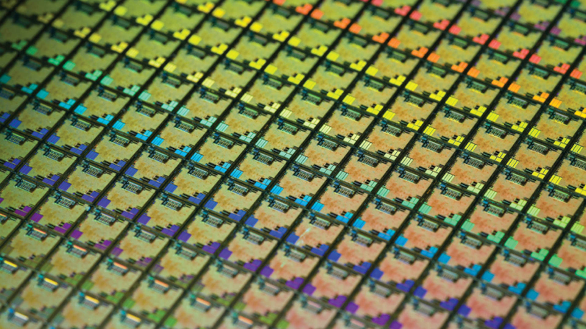
TSMC, the world’s leading semiconductor manufacturer, recently introduced its latest process technology, named A14. With dimensions of 14 angstroms (or 1.4 nanometers), this cutting-edge technology is particularly impactful in the domain of AI chip production.
Announced during TSMC’s North America Technology Symposium, the A14 process aims to accelerate AI transformation by providing enhanced computing speeds and improved power efficiency. TSMC continues to dominate the market, especially with growing interest in AI, making this announcement crucial for PC gamers waiting for the next generation of graphics and processing units.
According to TSMC, the A14 node is projected for launch in 2028. This new technology is expected to deliver up to a 15% performance boost at the same power consumption, or alternatively, reduce power needs by up to 30% without sacrificing speed. It also boasts over a 20% increase in logic density compared to previous nodes.
For gaming enthusiasts, the advancements in chip design and manufacturing will be vital as they can expect better performance from GPUs and CPUs powered by this technology. TSMC’s processes are critical for many leading brands, including Nvidia and AMD.
As this innovative A14 process approaches its release, the anticipation among tech aficionados grows, marking another exciting chapter in semiconductor development.