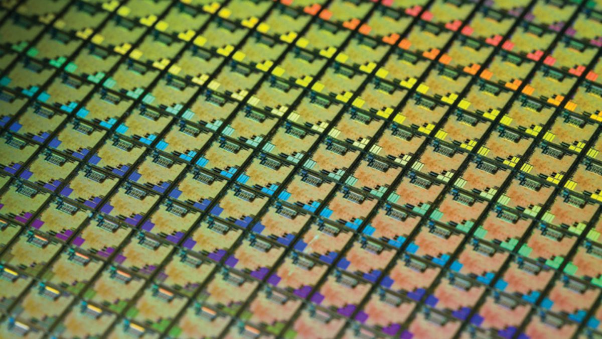
In a curious incident, a Reddit user stumbled across an entire silicon wafer near TSMC’s chip factory in Nanjing, China.
“Found this in a dumpster near TSMC fab, how to cut this into usable GPU?” - A comment from the Redditor.
The wafer was claimed to be fully intact, stirring conversations on how to repurpose it into functional GPUs, despite the wafer containing only test layouts, not actual designs.
It highlights discussions on chip binning — a testing process for silicon wafers — and raises questions about carelessness with potentially valuable resources.
Interestingly, many enthusiasts recommended using specialized tools, such as a clean room and a wire cutter, to handle the wafer safely. This incident not only showcases the enthusiasm of tech aficionados but also leads to speculations on the effluence at TSMC’s manufacturing sites.
To sum up, while the find may not lead to any new GPUs, it has certainly fueled interesting discussions and ambitions among those passionate about technology.